The problem
The client wanted 200 m of range, 0.2 m resolution under 10 m, a 50 Hz update rate, five hours on a single 21700 cell, a board under 80 cm2, a BOM under $150 and under 1 W of RF transmit power. The reference architecture in the same class tops out near 100 m on those constraints. Doubling range costs 12 dB of link budget. Sixteen times the transmit power breaks the 1 W limit, the thermal budget and the battery in one move. A bigger antenna breaks the board size and narrows the beam.
What I did
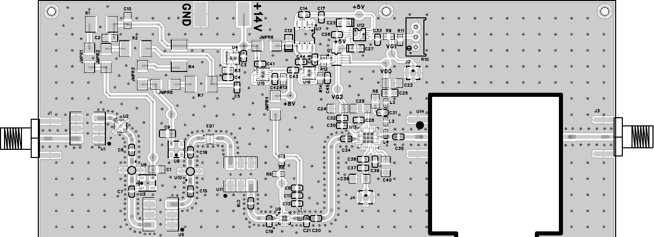
Two days of trade study landed on the receiver. The reference front end has a system noise figure near 13.5 dB, the transceiver chip's 11 to 12 dB plus 1.5 dB of antenna and routing loss. Putting a Mini-Circuits AVA-0233LN+ LNA first, between the antenna and a 24 GHz low pass filter, gives 17 dB of gain at 2.5 dB noise figure. By the Friis cascade the chip's noise figure divides down behind that gain, and the system lands near 4 dB.
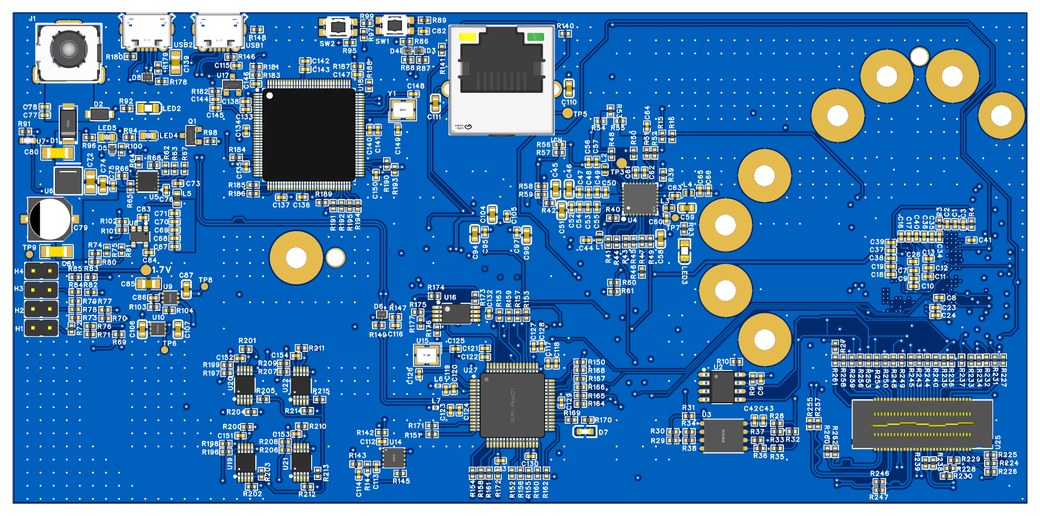
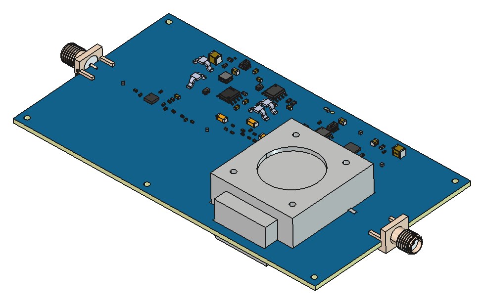
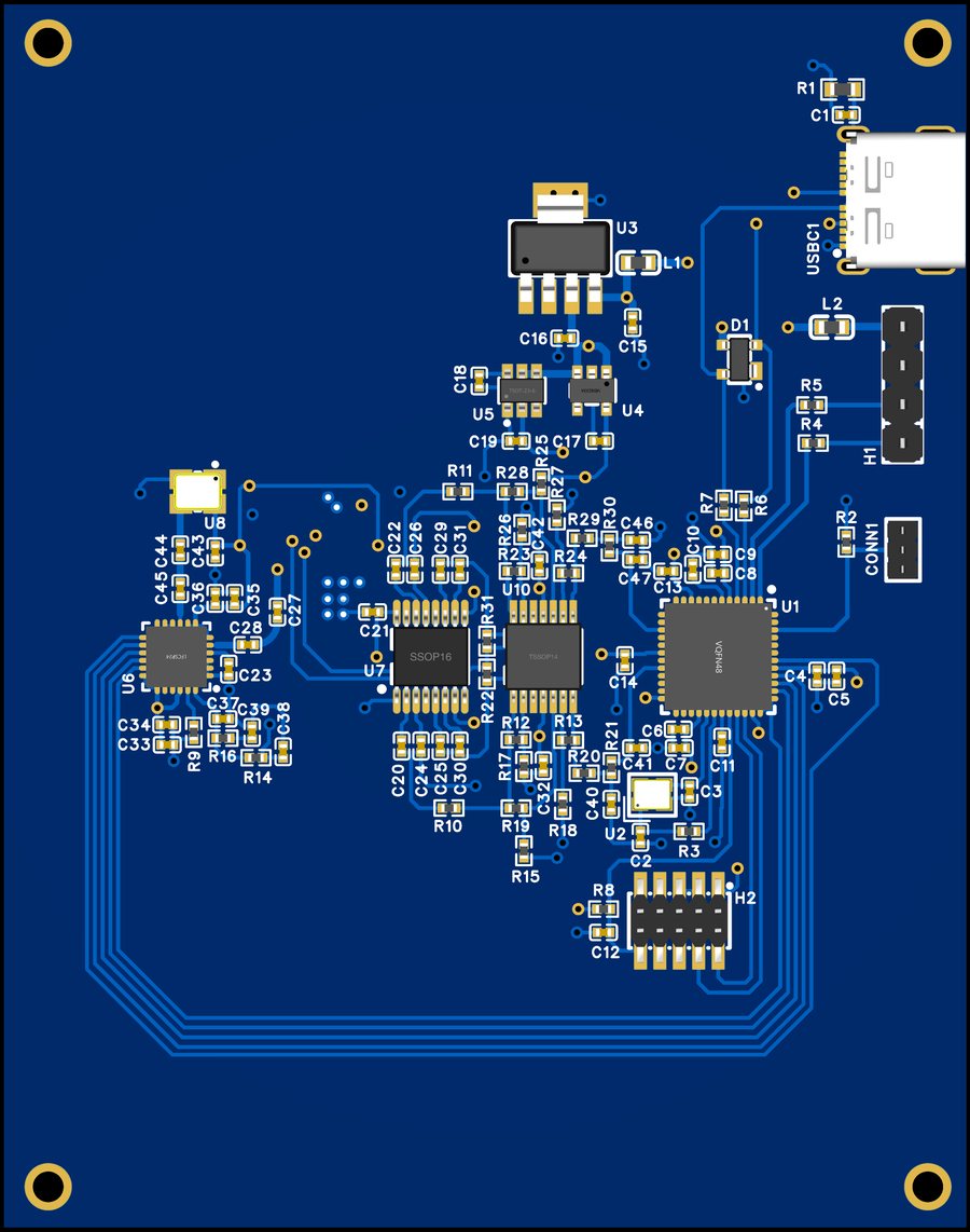
That is the 12 dB the doubling needs, with margin. The module is a single 10 by 8 cm board with the Infineon BGT24LTR11N16, the LNA, the filter and the microstrip patch antenna on one substrate. The LNA draws 65 mA at 5 V and the BOM stays under the cap. I wrote the range extension study so the client's RF reviewer could follow the link budget step by step.
Decisions that shaped it
- Spend the link budget on noise figure, not transmit power. Range goes as the fourth root of power, so the power path was never going to close.
- LNA before the filter. The first stage sets the cascaded noise figure.
- One board, no daughter card. The size and cost caps both punish a multi board build.
- A written study alongside the design, because a reviewer has to be able to check the move from 13.5 dB to 4 dB.
Result
200 m on the same cell, board and budget as a 100 m reference, with the reasoning written down.