The problem
The client had a system spec and a build slot at a contract manufacturer, but no amplifier design team. A single 10 W GaN part on its own is not the design. The chain needs a driver that brings the input up without adding noise the final stage then amplifies, an inter stage match that keeps the GaN linear until the spec power, and an isolator on the output so a mismatched antenna cannot reflect power back into the device. It also has to hold gain and P1dB across the supply window and the temperature range, because a PA that meets spec at 25 C and 22 V will not meet it at 70 C on a sagging supply.
What I did
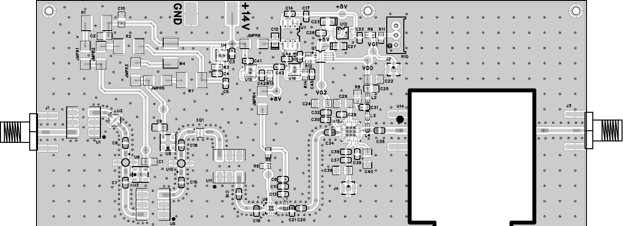
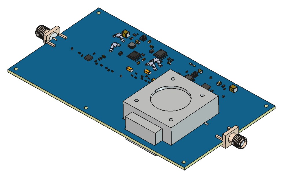
The chain is three stages. A Mini-Circuits PMA3-83LP+ driver, a fixed GAT series attenuator pad between the stages chosen from the small signal simulation, and a Qorvo QPA1019 GaN HEMT final stage biased at 22 V and 290 mA. A UIYBDI2528B isolator sits on the output. I simulated the whole chain in Keysight SystemVue with the vendor S-parameter files for every stage, verified the passive matching structures in ADS Momentum, and drew the layout in EasyEDA Pro so the schematic, Gerbers, BOM and pick and place all export from one project. The S-parameter set was swept at the temperature and supply corners so the manufacturer tests first articles against the same files I simulated.
Decisions that shaped it
- A fixed attenuator pad for the inter stage match instead of a tunable network. A 6 to 8 dB pad solves the small signal match and costs almost no board area.
- An isolator on the output rather than a circulator buried in the chain. Worst case reflected power lands in a 50 ohm load, not in the GaN.
- Corners swept in simulation, not just nominal. A PA that only meets spec at room temperature is not a deliverable.
- Machined heatsink path documented with the board so the thermal design is not left to the assembler.
Result
10 W across 5 to 6 GHz with gain and P1dB characterised at the corners, and nothing left for the contract manufacturer to guess.